|
CARME-M4 BSP
V1.5
|
|
CARME-M4 BSP
V1.5
|
FLASH driver modules. More...
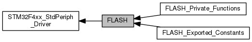
 Collaboration diagram for FLASH:
Modules | |
| FLASH_Exported_Constants | |
| FLASH_Private_Functions | |
Macros | |
| #define | SECTOR_MASK ((uint32_t)0xFFFFFF07) |
Enumerations | |
| enum | FLASH_Status { FLASH_BUSY = 1, FLASH_ERROR_RD, FLASH_ERROR_PGS, FLASH_ERROR_PGP, FLASH_ERROR_PGA, FLASH_ERROR_WRP, FLASH_ERROR_PROGRAM, FLASH_ERROR_OPERATION, FLASH_COMPLETE } |
| FLASH Status. | |
Functions | |
| void | FLASH_SetLatency (uint32_t FLASH_Latency) |
| Sets the code latency value. More... | |
| void | FLASH_PrefetchBufferCmd (FunctionalState NewState) |
| Enables or disables the Prefetch Buffer. More... | |
| void | FLASH_InstructionCacheCmd (FunctionalState NewState) |
| Enables or disables the Instruction Cache feature. More... | |
| void | FLASH_DataCacheCmd (FunctionalState NewState) |
| Enables or disables the Data Cache feature. More... | |
| void | FLASH_InstructionCacheReset (void) |
| Resets the Instruction Cache. More... | |
| void | FLASH_DataCacheReset (void) |
| Resets the Data Cache. More... | |
| void | FLASH_Unlock (void) |
| Unlocks the FLASH control register access. More... | |
| void | FLASH_Lock (void) |
| Locks the FLASH control register access. More... | |
| FLASH_Status | FLASH_EraseSector (uint32_t FLASH_Sector, uint8_t VoltageRange) |
| Erases a specified FLASH Sector. More... | |
| FLASH_Status | FLASH_EraseAllSectors (uint8_t VoltageRange) |
| Erases all FLASH Sectors. More... | |
| FLASH_Status | FLASH_EraseAllBank1Sectors (uint8_t VoltageRange) |
| Erases all FLASH Sectors in Bank 1. More... | |
| FLASH_Status | FLASH_EraseAllBank2Sectors (uint8_t VoltageRange) |
| Erases all FLASH Sectors in Bank 2. More... | |
| FLASH_Status | FLASH_ProgramDoubleWord (uint32_t Address, uint64_t Data) |
| Programs a double word (64-bit) at a specified address. More... | |
| FLASH_Status | FLASH_ProgramWord (uint32_t Address, uint32_t Data) |
| Programs a word (32-bit) at a specified address. More... | |
| FLASH_Status | FLASH_ProgramHalfWord (uint32_t Address, uint16_t Data) |
| Programs a half word (16-bit) at a specified address. More... | |
| FLASH_Status | FLASH_ProgramByte (uint32_t Address, uint8_t Data) |
| Programs a byte (8-bit) at a specified address. More... | |
| void | FLASH_OB_Unlock (void) |
| Unlocks the FLASH Option Control Registers access. More... | |
| void | FLASH_OB_Lock (void) |
| Locks the FLASH Option Control Registers access. More... | |
| void | FLASH_OB_WRPConfig (uint32_t OB_WRP, FunctionalState NewState) |
| Enables or disables the write protection of the desired sectors, for the first 1 Mb of the Flash. More... | |
| void | FLASH_OB_WRP1Config (uint32_t OB_WRP, FunctionalState NewState) |
| Enables or disables the write protection of the desired sectors, for the second 1 Mb of the Flash. More... | |
| void | FLASH_OB_PCROPSelectionConfig (uint8_t OB_PcROP) |
| Select the Protection Mode (SPRMOD). More... | |
| void | FLASH_OB_PCROPConfig (uint32_t OB_PCROP, FunctionalState NewState) |
| Enables or disables the read/write protection (PCROP) of the desired sectors, for the first 1 MB of the Flash. More... | |
| void | FLASH_OB_PCROP1Config (uint32_t OB_PCROP, FunctionalState NewState) |
| Enables or disables the read/write protection (PCROP) of the desired sectors. More... | |
| void | FLASH_OB_RDPConfig (uint8_t OB_RDP) |
| Sets the read protection level. More... | |
| void | FLASH_OB_UserConfig (uint8_t OB_IWDG, uint8_t OB_STOP, uint8_t OB_STDBY) |
| Programs the FLASH User Option Byte: IWDG_SW / RST_STOP / RST_STDBY. More... | |
| void | FLASH_OB_BORConfig (uint8_t OB_BOR) |
| Sets the BOR Level. More... | |
| void | FLASH_OB_BootConfig (uint8_t OB_BOOT) |
| Configure the Dual Bank Boot. More... | |
| FLASH_Status | FLASH_OB_Launch (void) |
| Launch the option byte loading. More... | |
| uint8_t | FLASH_OB_GetUser (void) |
| Returns the FLASH User Option Bytes values. More... | |
| uint16_t | FLASH_OB_GetWRP (void) |
| Returns the FLASH Write Protection Option Bytes value. More... | |
| uint16_t | FLASH_OB_GetWRP1 (void) |
| Returns the FLASH Write Protection Option Bytes value. More... | |
| uint16_t | FLASH_OB_GetPCROP (void) |
| Returns the FLASH PC Read/Write Protection Option Bytes value. More... | |
| uint16_t | FLASH_OB_GetPCROP1 (void) |
| Returns the FLASH PC Read/Write Protection Option Bytes value. More... | |
| FlagStatus | FLASH_OB_GetRDP (void) |
| Returns the FLASH Read Protection level. More... | |
| uint8_t | FLASH_OB_GetBOR (void) |
| Returns the FLASH BOR level. More... | |
| void | FLASH_ITConfig (uint32_t FLASH_IT, FunctionalState NewState) |
| Enables or disables the specified FLASH interrupts. More... | |
| FlagStatus | FLASH_GetFlagStatus (uint32_t FLASH_FLAG) |
| Checks whether the specified FLASH flag is set or not. More... | |
| void | FLASH_ClearFlag (uint32_t FLASH_FLAG) |
| Clears the FLASH's pending flags. More... | |
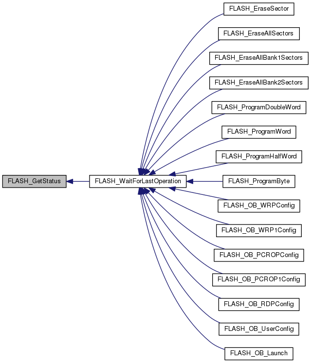
| FLASH_Status | FLASH_GetStatus (void) |
| Returns the FLASH Status. More... | |
| FLASH_Status | FLASH_WaitForLastOperation (void) |
| Waits for a FLASH operation to complete. More... | |
FLASH driver modules.
| void FLASH_ClearFlag | ( | uint32_t | FLASH_FLAG | ) |
Clears the FLASH's pending flags.
| FLASH_FLAG | specifies the FLASH flags to clear. This parameter can be any combination of the following values:
|
| None |
Definition at line 1481 of file stm32f4xx_flash.c.
| void FLASH_DataCacheCmd | ( | FunctionalState | NewState | ) |
Enables or disables the Data Cache feature.
| NewState | new state of the Data Cache. This parameter can be: ENABLE or DISABLE. |
| None |
Definition at line 306 of file stm32f4xx_flash.c.
| void FLASH_DataCacheReset | ( | void | ) |
Resets the Data Cache.
| None |
| None |
Definition at line 338 of file stm32f4xx_flash.c.
| FLASH_Status FLASH_EraseAllBank1Sectors | ( | uint8_t | VoltageRange | ) |
Erases all FLASH Sectors in Bank 1.
| VoltageRange | The device voltage range which defines the erase parallelism. This parameter can be one of the following values:
|
| FLASH | Status: The returned value can be: FLASH_BUSY, FLASH_ERROR_PROGRAM, FLASH_ERROR_WRP, FLASH_ERROR_OPERATION or FLASH_COMPLETE. |
Definition at line 586 of file stm32f4xx_flash.c.
Here is the call graph for this function:| FLASH_Status FLASH_EraseAllBank2Sectors | ( | uint8_t | VoltageRange | ) |
Erases all FLASH Sectors in Bank 2.
| VoltageRange | The device voltage range which defines the erase parallelism. This parameter can be one of the following values:
|
| FLASH | Status: The returned value can be: FLASH_BUSY, FLASH_ERROR_PROGRAM, FLASH_ERROR_WRP, FLASH_ERROR_OPERATION or FLASH_COMPLETE. |
Definition at line 653 of file stm32f4xx_flash.c.
Here is the call graph for this function:| FLASH_Status FLASH_EraseAllSectors | ( | uint8_t | VoltageRange | ) |
Erases all FLASH Sectors.
| VoltageRange | The device voltage range which defines the erase parallelism. This parameter can be one of the following values:
|
| FLASH | Status: The returned value can be: FLASH_BUSY, FLASH_ERROR_PROGRAM, FLASH_ERROR_WRP, FLASH_ERROR_OPERATION or FLASH_COMPLETE. |
Definition at line 505 of file stm32f4xx_flash.c.
Here is the call graph for this function:| FLASH_Status FLASH_EraseSector | ( | uint32_t | FLASH_Sector, |
| uint8_t | VoltageRange | ||
| ) |
Erases a specified FLASH Sector.
| FLASH_Sector | The Sector number to be erased. |
For STM32F42xxx/43xxx devices this parameter can be a value between FLASH_Sector_0 and FLASH_Sector_23.
For STM32F401xx devices this parameter can be a value between FLASH_Sector_0 and FLASH_Sector_5.
| VoltageRange | The device voltage range which defines the erase parallelism. This parameter can be one of the following values:
|
| FLASH | Status: The returned value can be: FLASH_BUSY, FLASH_ERROR_PROGRAM, FLASH_ERROR_WRP, FLASH_ERROR_OPERATION or FLASH_COMPLETE. |
Definition at line 437 of file stm32f4xx_flash.c.
Here is the call graph for this function:| FlagStatus FLASH_GetFlagStatus | ( | uint32_t | FLASH_FLAG | ) |
Checks whether the specified FLASH flag is set or not.
| FLASH_FLAG | specifies the FLASH flag to check. This parameter can be one of the following values:
|
| The | new state of FLASH_FLAG (SET or RESET). |
Definition at line 1450 of file stm32f4xx_flash.c.
| FLASH_Status FLASH_GetStatus | ( | void | ) |
Returns the FLASH Status.
| None |
| FLASH | Status: The returned value can be: FLASH_BUSY, FLASH_ERROR_PROGRAM, FLASH_ERROR_WRP, FLASH_ERROR_RD, FLASH_ERROR_OPERATION or FLASH_COMPLETE. |
Definition at line 1496 of file stm32f4xx_flash.c.
Here is the caller graph for this function:| void FLASH_InstructionCacheCmd | ( | FunctionalState | NewState | ) |
Enables or disables the Instruction Cache feature.
| NewState | new state of the Instruction Cache. This parameter can be: ENABLE or DISABLE. |
| None |
Definition at line 285 of file stm32f4xx_flash.c.
| void FLASH_InstructionCacheReset | ( | void | ) |
Resets the Instruction Cache.
| None |
| None |
Definition at line 327 of file stm32f4xx_flash.c.
| void FLASH_ITConfig | ( | uint32_t | FLASH_IT, |
| FunctionalState | NewState | ||
| ) |
Enables or disables the specified FLASH interrupts.
| FLASH_IT | specifies the FLASH interrupt sources to be enabled or disabled. This parameter can be any combination of the following values:
|
| None |
Definition at line 1418 of file stm32f4xx_flash.c.
| void FLASH_Lock | ( | void | ) |
Locks the FLASH control register access.
| None |
| None |
Definition at line 400 of file stm32f4xx_flash.c.
| void FLASH_OB_BootConfig | ( | uint8_t | OB_BOOT | ) |
Configure the Dual Bank Boot.
| OB_BOOT | specifies the Dual Bank Boot Option byte. This parameter can be one of the following values:
|
| None |
Definition at line 1242 of file stm32f4xx_flash.c.
| void FLASH_OB_BORConfig | ( | uint8_t | OB_BOR | ) |
Sets the BOR Level.
| OB_BOR | specifies the Option Bytes BOR Reset Level. This parameter can be one of the following values:
|
| None |
Definition at line 1263 of file stm32f4xx_flash.c.
| uint8_t FLASH_OB_GetBOR | ( | void | ) |
Returns the FLASH BOR level.
| None |
| The | FLASH BOR level:
|
Definition at line 1389 of file stm32f4xx_flash.c.
| uint16_t FLASH_OB_GetPCROP | ( | void | ) |
Returns the FLASH PC Read/Write Protection Option Bytes value.
| None |
| The | FLASH PC Read/Write Protection Option Bytes value |
Definition at line 1338 of file stm32f4xx_flash.c.
| uint16_t FLASH_OB_GetPCROP1 | ( | void | ) |
Returns the FLASH PC Read/Write Protection Option Bytes value.
| None |
| The | FLASH PC Read/Write Protection Option Bytes value |
Definition at line 1352 of file stm32f4xx_flash.c.
| FlagStatus FLASH_OB_GetRDP | ( | void | ) |
Returns the FLASH Read Protection level.
| None |
| FLASH | ReadOut Protection Status:
|
Definition at line 1365 of file stm32f4xx_flash.c.
| uint8_t FLASH_OB_GetUser | ( | void | ) |
Returns the FLASH User Option Bytes values.
| None |
| The | FLASH User Option Bytes values: IWDG_SW(Bit0), RST_STOP(Bit1) and RST_STDBY(Bit2). |
Definition at line 1299 of file stm32f4xx_flash.c.
| uint16_t FLASH_OB_GetWRP | ( | void | ) |
Returns the FLASH Write Protection Option Bytes value.
| None |
| The | FLASH Write Protection Option Bytes value |
Definition at line 1310 of file stm32f4xx_flash.c.
| uint16_t FLASH_OB_GetWRP1 | ( | void | ) |
Returns the FLASH Write Protection Option Bytes value.
| None |
| The | FLASH Write Protection Option Bytes value |
Definition at line 1324 of file stm32f4xx_flash.c.
| FLASH_Status FLASH_OB_Launch | ( | void | ) |
Launch the option byte loading.
| None |
| FLASH | Status: The returned value can be: FLASH_BUSY, FLASH_ERROR_PROGRAM, FLASH_ERROR_WRP, FLASH_ERROR_OPERATION or FLASH_COMPLETE. |
Definition at line 1280 of file stm32f4xx_flash.c.
Here is the call graph for this function:| void FLASH_OB_Lock | ( | void | ) |
Locks the FLASH Option Control Registers access.
| None |
| None |
Definition at line 951 of file stm32f4xx_flash.c.
| void FLASH_OB_PCROP1Config | ( | uint32_t | OB_PCROP, |
| FunctionalState | NewState | ||
| ) |
Enables or disables the read/write protection (PCROP) of the desired sectors.
| OB_PCROP | specifies the sector(s) to be read/write protected or unprotected. This parameter can be one of the following values:
|
| Newstate | new state of the Write Protection. This parameter can be: ENABLE or DISABLE. |
| None |
Definition at line 1133 of file stm32f4xx_flash.c.
Here is the call graph for this function:| void FLASH_OB_PCROPConfig | ( | uint32_t | OB_PCROP, |
| FunctionalState | NewState | ||
| ) |
Enables or disables the read/write protection (PCROP) of the desired sectors, for the first 1 MB of the Flash.
| OB_PCROP | specifies the sector(s) to be read/write protected or unprotected. This parameter can be one of the following values:
|
| Newstate | new state of the Write Protection. This parameter can be: ENABLE or DISABLE. |
| None |
Definition at line 1096 of file stm32f4xx_flash.c.
Here is the call graph for this function:| void FLASH_OB_PCROPSelectionConfig | ( | uint8_t | OB_PcROP | ) |
Select the Protection Mode (SPRMOD).
| OB_PCROP | Select the Protection Mode of nWPRi bits This parameter can be one of the following values:
|
| None |
Definition at line 1066 of file stm32f4xx_flash.c.
| void FLASH_OB_RDPConfig | ( | uint8_t | OB_RDP | ) |
Sets the read protection level.
| OB_RDP | specifies the read protection level. This parameter can be one of the following values:
|
| None |
Definition at line 1169 of file stm32f4xx_flash.c.
Here is the call graph for this function:| void FLASH_OB_Unlock | ( | void | ) |
Unlocks the FLASH Option Control Registers access.
| None |
| None |
Definition at line 936 of file stm32f4xx_flash.c.
| void FLASH_OB_UserConfig | ( | uint8_t | OB_IWDG, |
| uint8_t | OB_STOP, | ||
| uint8_t | OB_STDBY | ||
| ) |
Programs the FLASH User Option Byte: IWDG_SW / RST_STOP / RST_STDBY.
| OB_IWDG | Selects the IWDG mode This parameter can be one of the following values:
|
| OB_STOP | Reset event when entering STOP mode. This parameter can be one of the following values:
|
| OB_STDBY | Reset event when entering Standby mode. This parameter can be one of the following values:
|
| None |
Definition at line 1201 of file stm32f4xx_flash.c.
Here is the call graph for this function:| void FLASH_OB_WRP1Config | ( | uint32_t | OB_WRP, |
| FunctionalState | NewState | ||
| ) |
Enables or disables the write protection of the desired sectors, for the second 1 Mb of the Flash.
| OB_WRP | specifies the sector(s) to be write protected or unprotected. This parameter can be one of the following values:
|
| Newstate | new state of the Write Protection. This parameter can be: ENABLE or DISABLE. |
| None |
Definition at line 1016 of file stm32f4xx_flash.c.
Here is the call graph for this function:| void FLASH_OB_WRPConfig | ( | uint32_t | OB_WRP, |
| FunctionalState | NewState | ||
| ) |
Enables or disables the write protection of the desired sectors, for the first 1 Mb of the Flash.
| OB_WRP | specifies the sector(s) to be write protected or unprotected. This parameter can be one of the following values:
|
| Newstate | new state of the Write Protection. This parameter can be: ENABLE or DISABLE. |
| None |
Definition at line 974 of file stm32f4xx_flash.c.
Here is the call graph for this function:| void FLASH_PrefetchBufferCmd | ( | FunctionalState | NewState | ) |
Enables or disables the Prefetch Buffer.
| NewState | new state of the Prefetch Buffer. This parameter can be: ENABLE or DISABLE. |
| None |
Definition at line 263 of file stm32f4xx_flash.c.
| FLASH_Status FLASH_ProgramByte | ( | uint32_t | Address, |
| uint8_t | Data | ||
| ) |
Programs a byte (8-bit) at a specified address.
| Address | specifies the address to be programmed. This parameter can be any address in Program memory zone or in OTP zone. |
| Data | specifies the data to be programmed. |
| FLASH | Status: The returned value can be: FLASH_BUSY, FLASH_ERROR_PROGRAM, FLASH_ERROR_WRP, FLASH_ERROR_OPERATION or FLASH_COMPLETE. |
Definition at line 837 of file stm32f4xx_flash.c.
Here is the call graph for this function:| FLASH_Status FLASH_ProgramDoubleWord | ( | uint32_t | Address, |
| uint64_t | Data | ||
| ) |
Programs a double word (64-bit) at a specified address.
| Address | specifies the address to be programmed. |
| Data | specifies the data to be programmed. |
| FLASH | Status: The returned value can be: FLASH_BUSY, FLASH_ERROR_PROGRAM, FLASH_ERROR_WRP, FLASH_ERROR_OPERATION or FLASH_COMPLETE. |
Definition at line 710 of file stm32f4xx_flash.c.
Here is the call graph for this function:| FLASH_Status FLASH_ProgramHalfWord | ( | uint32_t | Address, |
| uint16_t | Data | ||
| ) |
Programs a half word (16-bit) at a specified address.
| Address | specifies the address to be programmed. This parameter can be any address in Program memory zone or in OTP zone. |
| Data | specifies the data to be programmed. |
| FLASH | Status: The returned value can be: FLASH_BUSY, FLASH_ERROR_PROGRAM, FLASH_ERROR_WRP, FLASH_ERROR_OPERATION or FLASH_COMPLETE. |
Definition at line 795 of file stm32f4xx_flash.c.
Here is the call graph for this function:| FLASH_Status FLASH_ProgramWord | ( | uint32_t | Address, |
| uint32_t | Data | ||
| ) |
Programs a word (32-bit) at a specified address.
| Address | specifies the address to be programmed. This parameter can be any address in Program memory zone or in OTP zone. |
| Data | specifies the data to be programmed. |
| FLASH | Status: The returned value can be: FLASH_BUSY, FLASH_ERROR_PROGRAM, FLASH_ERROR_WRP, FLASH_ERROR_OPERATION or FLASH_COMPLETE. |
Definition at line 753 of file stm32f4xx_flash.c.
Here is the call graph for this function:| void FLASH_SetLatency | ( | uint32_t | FLASH_Latency | ) |
Sets the code latency value.
| FLASH_Latency | specifies the FLASH Latency value. This parameter can be one of the following values:
|
| None |
Definition at line 248 of file stm32f4xx_flash.c.
| void FLASH_Unlock | ( | void | ) |
Unlocks the FLASH control register access.
| None |
| None |
Definition at line 385 of file stm32f4xx_flash.c.
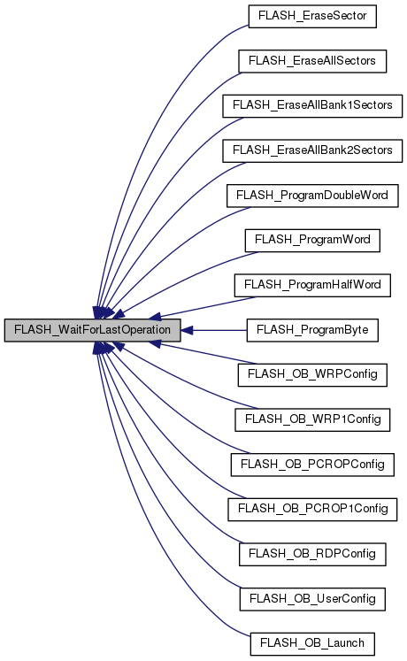
| FLASH_Status FLASH_WaitForLastOperation | ( | void | ) |
Waits for a FLASH operation to complete.
| None |
| FLASH | Status: The returned value can be: FLASH_BUSY, FLASH_ERROR_PROGRAM, FLASH_ERROR_WRP, FLASH_ERROR_OPERATION or FLASH_COMPLETE. |
Definition at line 1546 of file stm32f4xx_flash.c.
Here is the call graph for this function: Here is the caller graph for this function: 1.8.10